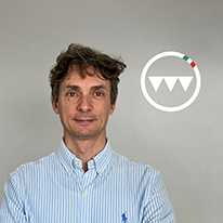
Monday Keynote Speaker

Raffaele Vallauri
VP Director
Technoprobe S.p.A. – Italy
Raffaele Vallauri, an accomplished executive with dual Italian and French nationality, was born in 1973. He holds a master’s degree in Materials Engineering from POLIMI University and he is completing an Executive MBA.
With a dynamic and versatile career spanning over two decades, Raffaele has worked for a few high-tech industries. Currently serving in Technoprobe Technology Team, he has been instrumental in increasing the company’s revenue. His leadership in innovation has led to the development and market introduction of cutting-edge MEMS products, earning him over 20 international patents.
His research interests include wafer probing, high mechanical strength and high conductivity materials. Raffaele has authored over 15 peer-reviewed publications. He is a member of the SWTest Technical Program Committee.
Raffaele is passionate about green energy and sustainability. Outside of his professional life, he enjoys swimming, trekking, and has a keen interest in meteorology. Known for his enthusiasm and positive outlook, Raffaele is always eager to explore new challenges and opportunities.
For more information, you can connect with Raffaele on LinkedIn (https://www.linkedin.com/in/raffaelevallauri/)
Mastering Emerging Probing Challenges: The Power of Agile and Continuous Innovation
The semiconductor industry is at a turning point, driven by AI, ultra-fine pitch devices, high-speed interfaces, and next-generation HBM. As wafer complexity grows, probe card vendors face unprecedented challenges: rapid innovation cycles, limited testing opportunities before deployment, and increasing performance demands.
This keynote explores how agile and lean development methodologies can transform probe card development, enabling vendors to iterate faster, collaborate earlier with customers, and deliver high-quality solutions in record time. By embracing concurrent engineering and MVP testing at customer sites, probe card vendors can significantly reduce time-to-market while ensuring cutting-edge reliability and performance. Together, we can turn emerging challenges into opportunities, driving the next wave of semiconductor innovation.
More information on the 2025 Keynote Speaker will be available soon
Thank you to our 2024 Keynote Speakers below!
Monday Keynote Speaker

Joe Parks, PhD
Vice President, Technology Development
Intel Corporation
Joe Parks, PhD, is the Vice President of Technology Development and Director of Intel’s Oregon Assembly Test Development Factory located in Portland, Oregon. His team is chartered to develop and deliver Intel’s cutting-edge Advanced Packaging and pre-assembly test technologies. These disaggregated wafer-level assembly technologies include 2.5D Embedded Bridge (EMIB), 3D solder-based Foveros die stacking technology, and 3D-3.5D Hybrid Bond Cu-Cu sub-10um interconnect technology. Additionally, his team develops all of Intel’s pre-packaged test processes including Automated Test Equipment, probing solutions, thermal control systems, probe card development and design, and factory automation. Notably, this includes Intel’s Singulated Die Test systems.
The OATD factory is a fully automated facility encompassing over 150k sq-ft of manufacturing space and generically supports process development, engineering samples, and initial ramp of both Intel and Foundry products. Joe has the honor of managing a highly competent, technical, and diverse team comprised of approximately 1400 people.
Known Good Die as a Key Enabler for Advanced Packaging in a Disaggregated World
Heterogeneous integration, or disaggregation, is quickly gaining importance as a means to drive Moore’s Law. Larger and more complex packages with a multitude of die, interposers, and silicon bridges are becoming prominent in segments like AI and HPC. Integrating multiple chiplets and creating complex die stacks via technologies such as Hybrid Bonding drives the need for true Known Good Die (KGD) validation prior to chip attach and package assembly. KGD improves yield and saves significant cost. As such, Sort has never been more critical to the Semiconductor industry as a means of screening bad chiplets via the shift of structural and functional content, as well as stress, upstream in the product’s manufacturing flow. Sort has always provided process feedback to the fab or foundry, but now has an additional role to play in providing timely and critical Wafer Level Assembly feedback. Intel has heavily leveraged advanced Sort, demonstrating significant yield and cost savings across multiple product segments with a first of a kind Singulated Die Sort (SDx) platform which enables testing die and die stacks with a unique and advanced thermal control system in High Volume Manufacturing. Advanced thermal control at Sort greatly improves the effectiveness of stress testing, enables a test content shift left and performance binning of die, and has a profound impact on the capture or attach rate of die to complex packages. Enabling test at the die and die stack level allows Wafer Bump, Die Prep, and Wafer Level Assembly health monitoring and yield learnings to pull in by months in the early critical stages of product development. Intel’s Die Sort capability is leading the way to enabling Known Good Die and Known Good Die Stacks to support advanced packaging and the disaggregated, chiplet future.
Tuesday Keynote Speaker

Joseph Roybal
Senior Vice President of Global Backend Operations
Wolfspeed, Inc.
Joseph Roybal is the Senior Vice President of Global Backend Operations at Wolfspeed aligning backend manufacturing roadmaps, production strategies, and capital allocation to scale efficiently with Wolfspeed’s exponential growth. He leads an expanding worldwide team focused on systemic manufacturing solutions, SiC package innovation, strategic partnerships with OSATs, and effective product manufacturing solutions for all Wolfspeed businesses and major SiC backend operations.
Packaging Trends in the Power Semiconductor Market
High Voltage (HV) power semiconductors play a critical role in the mass commercialization of electrical vehicles. Silicon carbide (SiC) based MOSFET’s have become commonplace as a superior alternative to silicon devices in HV applications.
While this shift to SiC devices results in significant attention on wafer substrates, epitaxial layers, and front end technology, it also results in increased focus on backend packaging requirements. Silicon carbide devices run at a higher junction temperature compared to silicon devices, which drives unique packaging trends and roadmaps.
Wolfspeed is leading the transformation from silicon to silicon carbide (SiC), and best-in-class packaging materials, equipment, and processes are needed to unlock the full potential of silicon carbide devices.
